Aisin Corporation's announcement of an artificial intelligence chip that reportedly consumes 98% less energy than conventional designs lands at a moment when the semiconductor industry's appetite for power has become its most pressing constraint.
The Japanese auto-parts manufacturer, best known for drivetrain components and transmissions, disclosed the development through Nikkei Asia, positioning itself alongside dedicated chipmakers in the race to make machine learning computationally sustainable.
The claim is striking in its scale: a near-total reduction in energy draw would reshape the economics of inference, the everyday workhorse of deployed AI systems.
On This Page
- The Strategic Context Behind Aisin's Energy-Efficient AI Chip
- How a 98% Energy Reduction Is Technically Achieved
- Reading the Disclosure Critically: What the Report Omits
- Implications for Japan's Semiconductor Ambitions
- What Independent Verification Would Require
- Broader Consequences for Sustainable AI Infrastructure
What makes the disclosure notable is not merely the number but the source. Aisin is a tier-one automotive supplier, not a fab operator or a design house in the conventional sense, and its entry into energy-efficient AI silicon signals how deeply semiconductor capability now penetrates industrial manufacturing.
Automotive firms increasingly need on-device intelligence for driver assistance, predictive maintenance, and sensor fusion, workloads where power budgets are tight and latency matters. A chip that slashes energy use could serve those embedded applications before it ever reaches a data centre.
The report, however, is deliberately thin. No performance benchmarks, no process node, no availability timeline, and no methodology for how the 98% figure was measured accompanied the announcement. That absence matters enormously in a field where energy-efficiency claims are notoriously sensitive to workload, precision, and comparison baseline.
This analysis examines what the disclosure implies, how such savings are typically achieved, and what independent verification would require before the claim can be treated as settled engineering fact.
TL;DR Aisin, a Japanese automotive components manufacturer, has developed an AI chip that reportedly cuts energy consumption by 98% compared with conventional designs, according to Nikkei Asia. The disclosure lacks benchmarks, process details, and measurement methodology, leaving the claim unverified but significant. The development reflects a broader industry pivot toward energy-efficient inference silicon, where power budgets increasingly constrain AI deployment in vehicles, edge devices, and data centres. Independent testing and technical disclosure will determine whether the figure holds under real workloads.
The Strategic Context Behind Aisin's Energy-Efficient AI Chip
Energy consumption has become the defining bottleneck of modern artificial intelligence, and the industry's response has shifted from raw performance to efficiency per operation. Data centres that once competed on floating-point throughput now publish power usage effectiveness figures and negotiate electricity contracts years in advance.
Against that backdrop, a 98% reduction claim commands attention because it addresses the single largest operating cost in deployed AI infrastructure.
Why Power Efficiency Now Determines Competitive Advantage
Training large models consumes megawatt-hours, but inference, the continuous execution of trained models in production, dominates lifetime energy use for most commercial systems. Every query answered, every image classified, and every sensor reading interpreted draws power, and those operations scale with user demand rather than one-time training budgets. Efficiency gains at inference therefore compound across millions of daily executions.
Regulatory pressure reinforces the economics. European and Japanese authorities increasingly require disclosure of data centre energy footprints, while grid operators in dense markets impose connection queues on new facilities.
A chip that delivers comparable throughput at a fraction of the power directly relieves those constraints, allowing operators to deploy more compute within fixed electrical envelopes.
The Automotive Supply Chain as an Unlikely Semiconductor Entrant
Aisin's core business supplies Toyota and other manufacturers with components engineered for durability and cost discipline rather than computational ambition. Its move into AI silicon reflects a broader convergence: vehicles are becoming sensor-dense computing platforms, and suppliers who control the electronics gain leverage over system integration and margin. Vertical integration into chips follows logically from that position.
Japanese industrial policy has actively encouraged this shift. Government-backed programmes subsidise advanced semiconductor development and encourage collaboration between automotive firms, research institutes, and foundries. Aisin's chip, whatever its eventual specifications, fits a national strategy of rebuilding domestic silicon capability after decades of decline in global market share.
How a 98% Energy Reduction Is Technically Achieved
A reduction of 98% is not incremental; it implies a fundamentally different computational approach rather than a refined version of existing designs. Conventional digital accelerators spend most of their energy moving data between memory and processing units, not performing arithmetic.
Architectures that eliminate or drastically shorten that movement can achieve order-of-magnitude savings, which is where the plausible explanations lie.
Analog and In-Memory Computing Architectures
Analog in-memory computing performs multiply-accumulate operations directly within memory arrays using physical properties such as conductance, avoiding the energy cost of shuttling weights between separate components. Research prototypes have demonstrated efficiency gains of two to three orders of magnitude for specific workloads, particularly matrix-vector multiplication in neural networks.
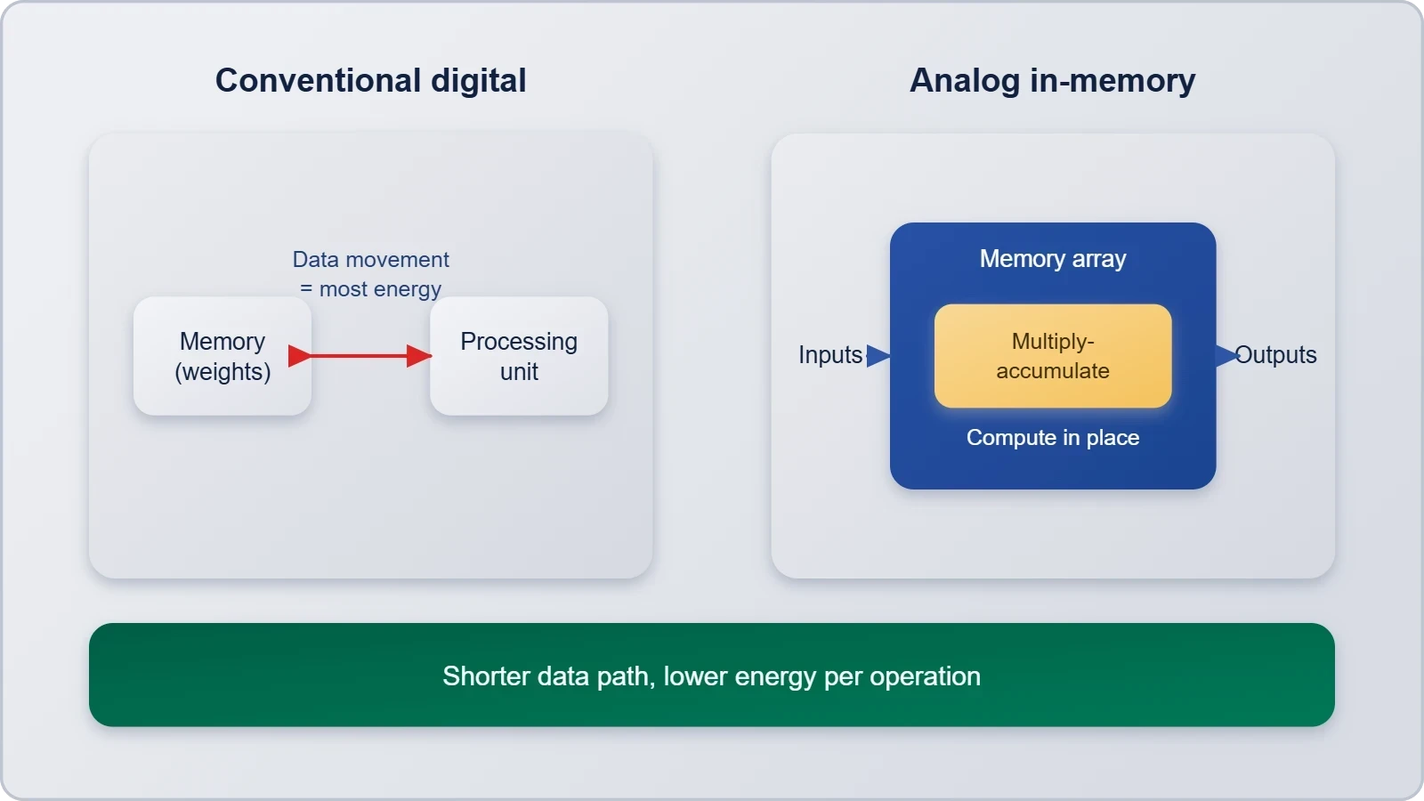
The trade-off is precision and programmability. Analog systems suffer from device variability, temperature sensitivity, and limited bit-depth, making them suitable for inference rather than training. If Aisin's chip employs such an approach, the 98% figure likely applies to a narrow class of operations rather than general-purpose AI processing.
Precision Reduction and Sparsity Exploitation
Digital designs can also approach extreme efficiency by lowering arithmetic precision and exploiting sparsity. Quantised neural networks operating at four-bit or lower precision consume dramatically less switching energy per operation, and architectures that skip zero-valued weights avoid computation entirely. Combined, these techniques can yield substantial savings on suitable models.
Such gains are real but conditional. They depend on model compatibility, retraining, and acceptance of accuracy loss, and they rarely apply uniformly across diverse workloads. A headline figure of 98% almost certainly reflects a best-case benchmark rather than average performance across the applications a customer would actually run.
Reading the Disclosure Critically: What the Report Omits
The Nikkei Asia report provides a single quantitative claim and little else, which places it in a familiar category of semiconductor announcements that generate headlines before technical substantiation. Responsible evaluation requires distinguishing between a demonstrated laboratory result, a projected design target, and a marketing figure derived from favourable assumptions. The absence of detail leaves all three possibilities open.
Benchmarking Standards and the Baseline Problem
Energy efficiency claims are meaningless without a stated baseline. A chip compared against a decade-old general-purpose processor will show enormous savings that shrink to modest proportions against a current dedicated accelerator. The choice of workload matters equally: sparse, low-precision inference on small models flatters efficiency metrics in ways dense training never would.
Established practice in the industry requires disclosure of throughput, latency, precision, model architecture, and power measurement methodology. Without those parameters, the 98% figure cannot be reproduced, compared, or audited. Independent evaluation by academic or standards bodies would be the appropriate next step before procurement decisions rest on the claim.
Distinguishing Laboratory Results from Commercial Products
Many semiconductor efficiency records originate in research prototypes fabricated at small scale, often in collaboration with academic laboratories. Translating those results into manufacturable products involves yield, reliability, and cost challenges that can erode efficiency advantages substantially. Aisin has not indicated whether its chip is a prototype, a design study, or a production-ready device.
Commercial availability timelines matter for competitive assessment. If the chip remains years from production, its impact on current energy consumption is negligible regardless of laboratory merit. The absence of any stated timeline in the report suggests the development is early-stage, which tempers immediate expectations while preserving long-term significance.
Implications for Japan's Semiconductor Ambitions
Japan once dominated global semiconductor production and has spent the past decade rebuilding capacity through subsidies, foundry partnerships, and research investment. Aisin's announcement, however thinly detailed, contributes to that narrative by demonstrating that Japanese firms outside the traditional chip sector are developing advanced silicon. The symbolic value may exceed the immediate technical one.
National Strategy and Industrial Policy
Tokyo has committed substantial public funds to semiconductor revitalisation, including support for advanced foundries and domestic design capability. Automotive electronics represent a natural niche where Japanese firms retain global strength, and energy-efficient AI chips for vehicles align industrial policy with commercial demand. Aisin's project fits neatly within that framework.
The strategic logic extends beyond individual firms. Reducing dependence on imported AI accelerators has become a policy priority across allied economies, and domestic capability in efficient inference silicon offers both supply security and technological sovereignty. Even partial success strengthens Japan's negotiating position in global technology supply chains.
Competitive Dynamics in the Global AI Chip Market
Established accelerator vendors dominate AI silicon through software ecosystems as much as hardware performance, and a new entrant faces steep barriers regardless of efficiency. Aisin's automotive focus may insulate it from direct competition with data centre giants, targeting embedded applications where ecosystem lock-in is weaker and customisation valued.
Should the efficiency claim prove reproducible, it would attract attention from edge computing vendors, industrial automation firms, and defence contractors seeking low-power inference. The competitive threat is less to market leaders than to other embedded AI suppliers, a narrower but commercially meaningful segment.
What Independent Verification Would Require
Turning a headline figure into accepted engineering knowledge demands transparency that the initial disclosure does not provide. The scientific method applies to industrial claims as much as academic ones: reproducibility, stated methodology, and independent measurement are the minimum conditions for credibility. Until those conditions are met, the 98% figure remains a claim rather than a finding.
- 01
- 02
- 03
- 04
Benchmarking Protocols and Peer Review
Credible evaluation would begin with publication of the chip's specifications, the models tested, and the power measurement setup. Standardised benchmarks such as MLPerf provide frameworks for comparing inference efficiency across hardware, and submission to such programmes would allow direct comparison with established accelerators.
Peer review adds a further layer of scrutiny, subjecting methodology to expert critique before results enter the technical literature. Companies with genuine breakthroughs typically pursue both routes, recognising that verified claims command higher prices and stronger customer trust than unverified announcements.
Commercial and Investor Implications of Unverified Claims
Investors and procurement officers face a familiar dilemma when confronted with dramatic but undocumented efficiency claims. Acting early risks capital misallocation if the figure fails scrutiny; waiting risks ceding advantage if it proves genuine. Prudent practice treats such announcements as signals of strategic direction rather than settled technical facts.
For Aisin specifically, the announcement serves multiple purposes regardless of verification outcome: it signals technological ambition to customers and partners, attracts research talent, and positions the firm within national semiconductor policy discussions. Those benefits accrue independently of whether the 98% figure survives independent testing.
Broader Consequences for Sustainable AI Infrastructure
The environmental footprint of artificial intelligence has moved from academic concern to boardroom agenda, with operators facing electricity costs, grid constraints, and reputational pressure simultaneously. Efficiency improvements of even modest scale, applied across millions of devices, produce aggregate savings that dwarf individual optimisations. The direction of travel matters more than any single announcement.
Energy Demand and Data Centre Constraints
Global data centre electricity consumption continues to rise, driven by AI workloads that require dense compute clusters and continuous operation. Grid operators in several regions have begun restricting new connections, forcing operators to seek efficiency gains or relocate to areas with surplus power. Silicon-level improvements directly address this constraint.
The relationship between efficiency and consumption is not straightforward, however. Cheaper computation historically increases total demand through rebound effects, as applications that were previously uneconomic become viable. A 98% efficiency gain could therefore expand AI deployment rather than reduce aggregate energy use, a dynamic worth monitoring.
The Road Ahead for Low-Power AI Silicon
Whatever the fate of Aisin's specific claim, the trajectory is clear: AI silicon must become dramatically more efficient for deployment to scale sustainably. Automotive, industrial, and edge applications will drive demand for chips that deliver adequate intelligence within tight power budgets, and suppliers who solve that problem will find ready markets.
Verification will separate durable contributions from transient announcements. Firms that publish methodology, submit to benchmarks, and welcome independent testing will build the credibility that sustains commercial relationships. The 98% figure may prove conservative, optimistic, or simply unverifiable, but the pressure that produced it will continue shaping semiconductor design for years.
From our network :
- Committed Mediterranean Precipitation Decline: Why Emissions Cuts Alone Cannot Restore Winter RainsNew NOAA research reveals that Mediterranean winter rains may decline irreversibly even with emissions cuts. Explore the science of committed climate change and regional impacts.
- Live Online English Classes for Kids: Do They Actually Reduce Anxiety?A ten-week study reveals that synchronous online English classes can significantly reduce child language anxiety while improving listening and reading skills. Discover what makes these programs effective and how parents can select the right one.
- The Final Descent: How ESA Retired the Legendary Cluster Constellation After 24 Years of Space Weather ScienceAfter 24 years mapping Earth’s magnetosphere, ESA’s Cluster mission concluded with a precisely controlled reentry over the South Pacific. This analysis explores the scientific legacy, engineering decisions, and debris mitigation principles behind one of space exploration’s most responsible retirements.
- How AI Agents Will Change the Way We Manage Personal FinancesExplore how AI agents are transforming personal finance through automated budgeting, bill payment, and investment management, while examining the critical security protocols and governance frameworks required for safe deployment.
- Mobile Learning and VR in English: What Global Evidence Reveals About Effective Language TechnologyA systematic review across 14 countries reveals which language-learning technologies genuinely work. Mobile learning, AI, and VR show measurable benefits when pedagogically integrated. This evidence-based guide helps educators and learners select technology that delivers real return on investment.
- Forbidden Matrix Patterns and Visible Lattice Points: A Geometric DictionaryExplore how multidimensional 0–1 matrices encode geometric truths, linking forbidden patterns to visible lattice points and hypergraph theory, with applications in combinatorics and computational geometry.
- The Hidden Cost of AI Convenience: Why Over-Permissioned Agents Are a Security Time BombDiscover why AI agents with excessive permissions create dangerous single points of failure, and learn how implementing least privilege principles can protect your organization from exploitation.
- CISA’s Ten-Advisory Wave: Why Generic Patching Fails in OT and How to Build Product-Specific PlaybooksCISA released ten ICS advisories in one week, exposing critical infrastructure risks. Generic patching fails in OT. Learn to build product-specific remediation playbooks.
- University Language Proficiency Exams: Why Institutional Tests Demand Different Preparation Than IELTS and TOEFLDiscover why university-specific language proficiency examinations differ fundamentally from IELTS and TOEFL, and learn strategic preparation approaches for institutional assessment success.
RESOURCES
- Japan's Aisin develops new type of AI chip that cuts energy use 98%asia.nikkei.com21 hours ago ... ... energy-efficient memory option. Aisin, a Toyota Motor supplier, developed the chip with Tohoku University in Sendai, tapping its MRAM…
- Aisin Develops Revolutionary AI Chip with 98% Lower Energy ...vibetrader.com17 hours ago ... Japanese automotive parts supplier Aisin has developed a ... Aisin's development of a 98% more energy-efficient AI chip using ...
- Environment | AISIN CORPORATION Global Websiteaisin.comAISIN Environmental Action Plan 2030 ; Scope 1 & 2 emissions 46.2% decrease compared to FY 2020 ; Promoting energy-saving activities with a focus…
- Tohoku University, Aisin develop AI chip with 65.7-millisecond startupjp.ibtimes.com1 day ago ... Part of the work resulted from commissioned research for Japan's New Energy and Industrial Technology Development Organization, the public ...
- Japan's Aisin develops AI chip that cuts energy use by 98%app.dealroom.co... power than similar existing chips, the company said Monday. The breakthrough is expected to help process large amounts of data more efficiently.
- MRAM-Info | MRAM Industry Portalmram-info.comTetsuo Endoh, together with Japan's automotive supplier Aisin, have developed what they say is the world's first 16 nm AI SoC with embedded STT-MRAM.…
- Japan Data Center Processor Market Size & Share Analysismordorintelligence.comJan 23, 2026 ... Aisin's edge AI chip co-developed with Tohoku improves power efficiency tenfold, while Denso's Data Flow Processor introduces a distinct ...
- Tohoku University and Toyota-supplier Aisin built a 16 nm AI chip ... - Xx.com18 hours ago ... ... energy savings. They used weight sharing and hybrid 8/16-bit math to ... Tohoku University: tohoku.ac.jp/japanese/2026/… jp.ibtimes.com.
- Idein AI Cast Smart Camera: Revolutionizing Retail Analytics | Hailohailo.aiEfficient processing icon – Hailo AI chip for Idein AI Cast camera. Consumer class product requiring operation in low temperature conditions. The low power ...
- The revolution of spintronics AI semiconductors that Tohoku ... - notenote.comJan 4, 2026 ... Chapter 3: What is so amazing about the "fusion" of Tohoku University and Aisin? Chapter 4: Japan going "outside" the…
- Marvell to Buy Lumentum for $115B, Tohoku Univ. - Tai - Mediumtai-semicon.medium.com20 hours ago ... Tohoku University and Aisin develop an AI chip with embedded MRAM ... AI system faster and more energy-efficient. Nagasaki is…
- The University of Tokyo, AISIN and other organizations jointly ...sj.jst.go.jpFeb 21, 2024 ... Science Japan publishes news and stories about Japan's leading research institutions and their findings and achievements.
- AI Infrastructure News | Broadcombroadcom.com... AI Chip Demand. Advanced Substrate Technologies (AST) today announced ... power-efficient solutions for gigawatt-scale AI clusters. AI Infrastructure.
- Tohoku University and Aisin Develop AI Chip That Boots About 39x ...xenospectrum.com1 day ago ... ... chip memory, improving efficiency in both memory bandwidth and power consumption. OS boot about 39x faster, AI inference energy…
- Aisin's Arm-Based AI Chip Skips DRAM and Boots 39x Fasterfourweekmba.com8 hours ago ... A 16nm AI chip from Tohoku University and Toyota group parts maker AISIN boots its operating system 65.7 milliseconds after…
- 01
- 02
- 03
- 04
- 05
- 06
- 07
- 08
0 Comments